Overview
One of the often neglected necessities of synchrotron radiation
science is detector technology. The Gruner
Detector Group designs and builds novel detectors for various
applications including macromolecular x-ray crystallography,
microcrystallography, x-ray tomography, and electron microscopy. Our
design goals include high-speed imaging, high spatial resolution,
wide dynamic range, compatibilty with femtosecond signal pulses, and
high application versatility for storage ring, energy recovery
linac, and x-ray free electron laser synchrotron sources, as well as
for non-synchrotron sources. See below for
a list of current projects.
Pixel Array Detectors
Pixel Array Detectors (PADs) are being developed by the Detector
Group to meet the x-ray detection needs of the synchrotron
community. In overview, a PAD is an application-specific integrated
circuit (ASIC) coupled to a diode detector via bump-bonding. The
ASIC offers a flexible platform for development, as well as
a greater potential for high speed imaging via commercial
grade mixed-mode CMOS circuits. In addition, the diode itself
directly converts absorbed x-rays into electron hole pairs, which
are swept into the ASIC for processing by an applied electric field.
Compared to common scintillator-based imaging arrays that must
detect secondary photons produced by the scintillation material, a
PAD's direct detection method offers much better signal-to-noise
ratios and spatial resolution.
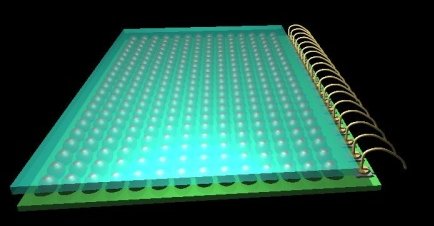
To the right is a basic illustration of a PAD
chip (not to scale). The top layer (blue) is the diode used
for converting absorbed x-rays to charge. The diode is
typically silicon, but other materials with shorter
absorption lengths (e.g. GaAs) can be used for more
efficient detection of harder x-rays. The bottom layer
(green) is the CMOS ASIC. This is an application-specific
integrated circuit custom-made to the requirements of the
experiment. The diode and the ASIC are mated using
bump-bonds (represented by the balls between the the two).
On the right hand side of the detector the I/O to the ASIC
is seen. The dimensions of the detector pixels depend
heavily on the application; typical values are between 100
and 200 microns on a side.
CCD detector technology that resulted from earlier work by
the group is in use at every hard x-ray synchrotron source
in the world. PADs resulting from work by the group have
been or are being used at synchrotron x-ray sources around
the world.
|
 Basic illustration of a
PAD chip Basic illustration of a
PAD chip |
Pixel Array Detectors
LCLS CSPAD
The Cornell-SLAC pixel array detector (CSPAD) is the
first PAD designed for a hard X-ray Free Electron Laser (XFEL),
developed for use at at SLAC (Linac Coherent
Light Source (LCLS)). Variants of the CSPAD now serve as the
primary detectro instruments at the LCLS.
An XFEL produces femtosecond pulses of coherent x-rays with fluxes
that are orders of magnitude above that produced with other
man-made x-ray sources. Since the x-rays from each pulse arrive in
femtoseconds, photon counting PADs were not useful, and a Cornell
integrating PAD design was chosen. The CSPAD achieved a
signal-to-noise ratio of 8 and a dynamic range of >2500 for 8
keV x-rays. The detector was designed as a 3-side buttable chip of
194x185 pixels, each 110 microns on a side.
The Gruner group designed and
fabricated the CSPAD chips, while SLAC built them into large
detectors. Three full scale detectors (1516x1516 pixels) and
about a half dozen 758x758 pixel detectors are now operational
at the LCLS.
References: 225, 243,
246, 267, 274, 282, 28f; SLAC
publication
Mixed Mode PAD (MMPAD)
This detector is designed to have
a very wide dynamic range without losing single x-ray sensitivity.
This is done by designing a pixel that has combined analog and
digital character, hence the name mixed-mode PAD. The scheme is to
use an architecture with noise that may grow, but is always much
less than the equivalent shot noise in the x-ray signal.
The current MMPAD detector is a 3-side buttable detector of
128x128 pixels, each 150 microns on a side. It has a SNR of about
6 for 8 keV x-rays, frames at 1 kHz, and has a dynamic range of
>3x10⁷ x-rays per pixel per frame. A 2x3 module
detector is already in use at Cornell, and more are being built.
Currently the chip is being mechanically redesigned to allow
assembly of arbitrarily many chips into a mosaic with chip gaps of
only a few millimeters. The MMPAD is also being adapted for use in
electron microscopy.
An even wider dynamic range version, the Hihg Dynamic Range PAD
(HDR-PAD) is being developed.
References: 196, 226,
265, 281, 289,
294, 301, 302, 308, 317, 319, 25f, 28f
Keck PAD
Designed for microsecond time-resolved
X-ray imaging, this PAD is the
successor to the well-known 100x92 prototype PAD that has been
used for fuel injector and reactive metal foil research. It was
designed for single bunch imaging at the APS with successive
full-frame (14-bits) images every 150 ns, and even faster for
fewer bits.
The Keck PAD is
designed to capture a frame every ~150 ns. It uses an
integrating architecture to store the
signal of eight successive frames on an on-chip,
per-pixel, array of holding capacitors. A
16x16 pixel chip has already been tested; construction of a 2x3
array of 128x128 pixel chips is underway.
References: 205, 250,
264,303,318,322, 28f
FPGA PAD
This PAD is being designed to move functionality from hardware
into firmware. The idea is to mate a FPGA to each PAD ASIC
(application-specific integrated circuit) via a wide-bandwidth
pathway. The functionality of the ASIC depends on the firmware in
the FPGA. Thus, a single ASIC can accomplish different PAD
functions.
References: 284
Electron Microscope PAD (EM-PAD)
This is a variant of the MM-PAD adapted for use as the detector in
scanning transmission electron microscopy (STEM). It allow rapid
data collection of the full 4-dimentional diffraction patterns of
objects in STEM mode. It also enables all the standard STEM
microscopies.
References: 242, 320,
323, 328, 329
General Detector Considerations
and PADs for Hard (> 15 keV) X-ray Imaging
References: 216, 258,
287, 290, 306, 311, 314, 315
sCMOS X-ray detector
The sCMOS detector was developed for high spatial resolution, high
energy applications. It is a small (5mm x 5mm) detector capable of
expanding into a large format, with <10 micron resolution and
good detection efficiency for x-rays in the 25-100keV range. It uses
scintillating fiber optics to convert x-rays to length so as to have
high x-ray stopping power while preserving spatial resolution. A
fiber-optic magnifying taper couples the initial optics to a sCMOS
chip.
References: 253, 291,
31f
Direct Detection CCD
This detector is a large area (10 cm x 10 cm), large format (4k x 4k
pixels) direct detection charge-coupled device (CCD) for
macromolecular crystallography. This is a relatively inexpensive
alternative to PADs that will outperform phosphor-coupled CCDs in
low flux applications, such as microcrystallography.
The detector consists of a CCD
structure on the front-side of a thick Si high-resistivity wafer.
The wafer is back-biased to fully deplete it so the entire
thickness of the wafer is sensitive to x-rays; this provides good
x-ray stopping power up to 20 keV. Each stopped x-ray produces
thousands of electron-hole pairs. While this quickly fills the
pixel well-depth, limited to about 106 electrons,
thereby limiting x-rays stored to each pixel to a few hundred, the
signal per x-ray should greatly exceed the per pixel read noise,
so the detector quantum efficiency should be excellent. To
compensate for the limited well-depth, the CCD is divided into 16
ports that all read out in parallel at high speed.
The final device frames at 2-5 Hz
with noise low enough to see single 12 keV x-rays. The
direct-detection CCD performs competitively with the more common
phosphor-coupled fiberoptic taper CCD detectors.
References: 293,
32f
- Sol
M. Gruner, Professor of Physics, smg26@cornell.edu
- Mark
W. Tate, Senior Research Associate, mwt5@cornell.edu
- Hugh
Philipp, Senior Research Associate, htp2@cornell.edu
- Darol
Chamberlain, CHESS Research Support Specialist, dc35@cornell.edu
- Marianne Hromalik, Visiting Professor, SUNY Oswego, msp44@cornell.edu
- Prafull Purohit, Research Support Specialist and Graduate
Student, prafull.purohit@cornell.edu
- Kate Shanks, Postdoctoral Associate, ksg52@cornell.edu
- Joel Weiss, PhD Candidate, jtw93@cornell.edu
- Julian Becker, Postdoctoral Associate, julian.becker@cornell.edu
PADs in the Press
Shock Wave Movies
Last updated 2016-10-26 SMG